TSMC: Importance of Open Innovation Platform Is Growing, Collaboration Needed for Next-Gen Chips
by Anton Shilov on October 12, 2023 8:00 AM EST
This year TSMC is commemorating 15 years of its Open Innovation Platform, a multi-faceted program that brings together the foundry's suppliers, partners, and customers to help TSMC's customers better build innovative chips in an efficient and timely manner. The OIP program has grown over the years and now involves tens of companies and over 70,000 IP solutions for a variety of applications. It continues to grow, and its importance will get higher than ever when next generation technologies, such as 2 nm, and advanced packaging methods become mainstream in the coming years.
"This is not a marketing program, it is actually an engineering program to enable the industry," said Dan Kochpatcharin, Head of Design Infrastructure Management at TSMC, at the OIP 2023 conference in Amsterdam, the Netherlands. "We have a huge engineering team behind to work with the EDA partners, IP partners, and design partners."
Shrinking Time-to-Market
Speeding up time-to-market is one of the corner stones of TSMC's OIP program. Before emergence of the OIP program in 2008, TSMC would develop a process technology and process development kits (PDKs) in about 18 months time, then hand over PDKs and design rules to its partners among electronic design automation (EDA) software and IP developers. The latter would spend another 12 months creating EDA tools and building IP blocks before supplying programs and IP solutions to actual chip designers. Then it would take chip developers another 12 months to build actual chips.
With OIP, TSMC's EDA tool and IP design partners can start development of their products a few months after TSMC begins development of its new production node. And, by the time TSMC finalizes its process technology, EDA tools and IP are ready for chip designers, the foundry claims. This speeds up time-to-market by about 15 months, TSMC says. Meanwhile, as development time for new nodes is stretching and so is development time for chips, the value of early collaboration between TSMC and EDA and IP providers is increasing.
For example, TSMC has been working with its partners on N2 (2nm-class) EDA and IP readiness for two years now, with TSMC aiming to have tools and common IP ready for chip designers in H2 2025.
Quality Matters
An avid reader would wonder why, even with the success of the program, OIP only grew to 39 IP members in 15 years. As it turns out, TSMC is extremely picky with companies that join the program, according to Dan Kochpatcharin. TSMC needs members of the OIP program to really contribute to it and make the joint effort something bigger than the sum of all parts. Because TSMC clients use IP, software, and services offered by participants of the OIP program, the latter have to be really good in their fields to be a part of OIP.
In fact, TSMC even has its TSMC9000 program (the name mimics ISO 9000 quality policy) that sets quality requirements for IP designs. IP collaborators undergo TSMC9000 evaluations, with results available on TSMC-Online, guiding customers on IP reliability and risks.
"We do a lot of qualifications for IP, before the test shuttles they do tape outs, and then they have TSMC 9000 checklists, […] customer can see [all] the results on TSMC-Online," explained Kochpatcharin. "So, they can see okay, this IP got silicon introductions, so, they have more confidence in the IP. [They also see] how many customers adopted [this IP], how many tape outs, and how many productions. For the lack of a better term, Consumer Report for IP."
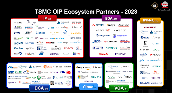
Alliance members list their IPs in TSMC's premier catalog, which features thousands of IP options from 39 contributors. Customers can search for IPs using the 'IP Center' on the TSMC-Online Design Portal. Each IP in the catalog is developed, sold, and supported by its originating partner. Meanwhile, chip developers can even check out how popular is one IP or another, which can give chip developers some more confidence in their choice. Confidence is something important today and will be even more important for 3 nm, 2 nm, and future nodes as tape outs get more expensive.
Six Alliances
But speeding up time-to-market and ensuring quality are not the only purposes of the OIP program. It is meant to simplify development, production, testing, and packaging of chips. TSMC's OIP involves a variety of members and is organized into six programs or alliances, each responsible for a separate line of work:
- IP Alliance that that is focused on providing silicon-verified, production-proven and foundry-specific intellectual property (IP) that TSMC customers can choose from.
- EDA Alliance that includes companies which offer electronic design automation (EDA) software that is compliant with TSMC technology requirements and support the foundry's production nodes.
- Design Center Alliance which comprises of contract chip designers as well as companies offering system level design solution enablement.
- Cloud Alliance that combines EDA toolmakers and cloud service providers enabling TSMC's customers to develop and simulate their chips in the cloud to reduce in-house compute needs.
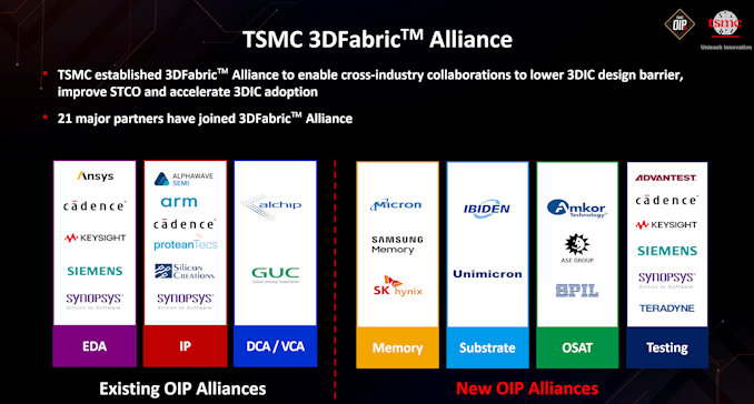
- 3D Fabric Alliance that unites all companies responsible for advanced packaging as well as development of multi-chiplet processors, which essentially includes all of the abovementioned companies as well as makers of memory (including Micron, Samsung, and SK Hynix), substrates, OSATs, and makers of test equipment.
- Value Chain Alliance that resembles Design Center Alliance, but is meant to offer a broader range of contract chip design services and IP offerings to cater to needs of a broad range of customers spanning from startups and OEMs to ASIC designers.
The 3D Fabric Alliance program was introduced late last year, so it can be considered the newest addition to OIP. Meanwhile, 3DFabric Alliance looks to be expanding fast with new members and for a reason.
Multi-Chiplet Designs Become New Standard
Process technologies are getting more complex, and this is not going to change. Chip design workflow might get a little easier going forward as EDA makers like Ansys, Cadence, Siemens EDA, and Synopsys are incorporating artificial intelligence capabilities into their tools. But because High-NA EUV lithography scanners halve reticle size from 858 mm2to 429 mm2, it looks like the majority of AI and high-performance computing (HPC) processors are going to adopt multi-tile design in the coming years, which will drive the need for software that assists creation of multi-tile solutions, advanced packaging, HBM-type memory, and all-new methods of testing. This will again increase importance of industry-wide collaboration and the importance of TSMC's OIP.
"[We have offered InFO_PoP] and InFO_oS 3D IC since 2016, [3D ICs have been] in production for years already, [but] back then it was still a niche [market]," said Kochpatcharin. "The customer had to know what they were doing […] and only a few people could do a 3D IC [back then]. [In] 2021 we launched the 3DFabric activity, we wanted to make it generic for everybody because with AI and HPC coming [from multiple companies], [these] cannot be niche things anymore. So, everybody has to be able to use 3D IC. [For example], automotive is a wonderful [application for] 3D IC, there is a [huge] market out there."
Meanwhile, to enable next-generation connectivity between chips and between chiplets, TSMC envisions silicon photonics will be needed, so the company is actively working in this direction within its OIP program.
"If you go to N2 and the next one coming up is silicon photonics," said Kochpatcharin. "This is where we launched a process needed to have [design service partners] to be able to support the customer."


4 Comments
View All Comments
littlebitstrouds - Thursday, October 12, 2023 - link
Spends years locking innovation under monopolistic principals... suddenly group think might take over: OMG we need to open source the future!!!It's wild to think where we'd be if these things were actually implemented from the beginning. Reply
Yojimbo - Thursday, October 12, 2023 - link
Far behind... Not likely to get a disruptive effort when one can't make more money doing it. Chips and chipmaking are not a community utility like operating systems are. ReplyThreska - Thursday, October 12, 2023 - link
The need for money is easier to ignore in open source. Capital intensive chip endeavors, not so much. Replymeacupla - Thursday, October 12, 2023 - link
Disagree. Chips have become a necessary part of society. They are so important now, that governments will pay companies to build fabs in their country. Reply