Packaging
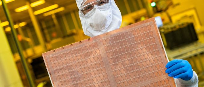
Although Intel’s annual Innovation event doesn’t kick off until tomorrow, the company is already publishing some announcements ahead of the show – and it’s not the trivial stuff, either. This morning the company is showing off their initial work on developing a glass core substrate and associated packaging process for their chips. As a result of their progress with research and development on the glass cores, Intel is now planning on introducing glass core substrates to its products in the second half of this decade, allowing them to package chips in more complex, and ultimately higher-performing configurations. There’s a lot to unpack from Intel’s relatively short announcement, but at a high level, glass core substrates have been under research for over a decade as a...
TSMC: Short Supply of HPC GPUs to Persist for 1.5 Years
The reports about an insufficient supply of compute GPUs used for artificial intelligence (AI) and high-performance computing (HPC) servers became common in recent months as demand for GPUs to...
6 by Anton Shilov on 9/7/2023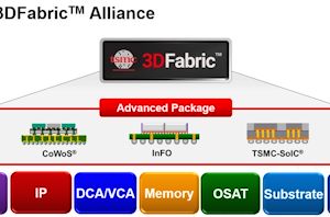
TSMC to Build $2.87 Billion Facility For Advanced Chip Packaging
TSMC on Tuesday announced plans to construct a new advanced chip packaging facility in Tongluo Science Park. The company intends to spend around $2.87 billion on the fab that...
3 by Anton Shilov on 7/25/2023
Out With Organic, In With Glass? DNP Unveils Glass Core Substrate Tech For Chips
As the chip industry develops more sophisticated processors with higher heat dissipation requirements, some firms have moved on to chiplet-based designs. This not-so-gradual shift has resulted in chip packaging...
17 by Anton Shilov on 3/23/2023UCIe Consortium Incorporates, Adds NVIDIA and Alibaba As Members
Among the groups with a presence at this year’s Flash Memory Summit is the UCIe Consortium, the recently formed group responsible for the Universal Chiplet Interconnect Express (UCIe) standard...
21 by Ryan Smith on 8/4/2022Universal Chiplet Interconnect Express (UCIe) Announced: Setting Standards For The Chiplet Ecosystem
If there has been one prominent, industry-wide trend in chip design over the past half-decade or so, it has been the growing use of chiplets. The tiny dies have...
25 by Ryan Smith on 3/2/2022
AMD: We’re Using an Optimized TSMC 5nm Process
When AMD started using TSMC’s 7nm process for the Zen 2 processor family that launched in November 2019, one of the overriding messages of that launch was that it...
44 by Dr. Ian Cutress on 1/10/2022
Intel's Process Roadmap to 2025: with 4nm, 3nm, 20A and 18A?!
In today’s Intel Accelerated event, the company is driving a stake into the ground regarding where it wants to be by 2025. CEO Pat Gelsinger earlier this year stated...
326 by Dr. Ian Cutress on 7/26/2021_carousel.jpg)
Intel Accelerated Webcast on July 26th: Update on Process Technology and Roadmaps
Earlier this year, new Intel CEO Pat Gelsinger outlined his new ‘IDM 2.0’ vision for Intel. This vision was a three pronged strategy based on improving its own process...
32 by Dr. Ian Cutress on 7/12/2021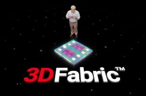
3DFabric: The Home for TSMC’s 2.5D and 3D Stacking Roadmap
Interposers. EMIB. Foveros. Die-to-die stacking. ODI. AIB.TSVs. All these words and acronyms have one overriding feature – they are all involved in how two bits of silicon physically connect...
9 by Dr. Ian Cutress on 9/2/2020_carousel.jpg)
Intel Next-Gen 10-micron Stacking: Going 3D Beyond Foveros
One of the issues facing next-generation 3D stacking of chips is how to increase the density of the die-to-die interface. More connections means better data throughput, reducing latency and...
32 by Dr. Ian Cutress on 8/14/2020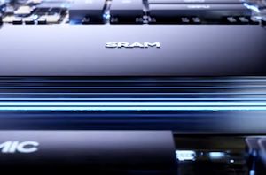
Samsung Announces "X-Cube" 3D TSV SRAM-Logic Die Stacking Technology
Yesterday, Samsung Electronics had announced a new 3D IC packaging technology called eXtended-Cube, or “X-Cube”, allowing chip-stacking of SRAM dies on top of a base logic die through TSVs. Current...
21 by Andrei Frumusanu on 8/14/2020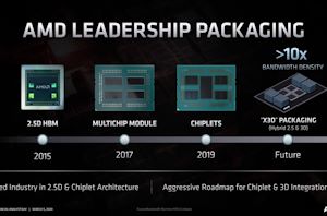
AMD Discusses ‘X3D’ Die Stacking and Packaging for Future Products: Hybrid 2.5D and 3D
One of AMD’s key messages at its Financial Analyst Day 2020 is that the company wants to remain on the leading edge when it comes to process node technology...
12 by Dr. Ian Cutress on 3/5/2020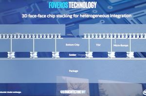
Intel's Interconnected Future: Combining Chiplets, EMIB, and Foveros
While Intel works on getting its main manufacturing process technology on track, it is spending just as much time and effort in researching and developing the rest of the...
117 by Dr. Ian Cutress on 4/17/2019


