Original Link: https://www.anandtech.com/show/20046/intel-unveils-meteor-lake-architecture-intel-4-heralds-the-disaggregated-future-of-mobile-cpus
Intel Unveils Meteor Lake Architecture: Intel 4 Heralds the Disaggregated Future of Mobile CPUs
by Gavin Bonshor on September 19, 2023 11:35 AM EST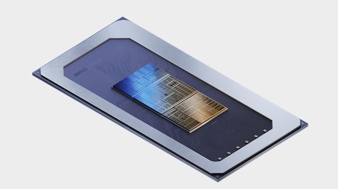
During the opening keynote at Intel's Innovation event in San Jose, Chief Executive Officer Pat Gelsinger unveiled a score of details about the upcoming Meteor Lake client platform. Intel's Meteor Lake marks the beginning of a new era for the chipmaker, as they move away from the chaotic Intel 7 node and go into a rollout of their Foveros 3D packaging with EUV lithography for their upcoming client mobile platform. Meteor Lake uses a tiled, disaggregated chiplet architecture for its client-centric processors for the first time, changing the very nature of Intel's consumer chips going forward. And, according to Intel, all of these changes have allowed them to bring some significant advancements to the mobile market.
Intel's first chiplet-based consumer CPU breaks up the common functions of a modern CPU into four individual tiles: compute, graphics, SoC, and an I/O tile. Within the makeup of the compute tile is a new pair of cores, a P-core named Redwood Cove and a new E-core called Crestmont. Both these cores promise IPC gains over their previous counterparts, but perhaps the most interesting inclusion is a new type of E-core embedded directly into the SoC tile, which Intel calls 'Low Power Island.' These new LP E-cores are designed with the idea that light workloads and processes can be taken off the more power-hungry compute tile and offloaded onto a more efficient and lower-powered tile altogether. Other major additions include a first-for-Intel Neural Processing Unit (NPU), which sits within the SoC tile and is designed to bring on-chip AI capabilities for workloads and inferencing, paving the way for the future.
With Meteor Lake, Intel is aiming to put themselves in a more competitive position within the mobile market, with notable improvements to compute core hierarchy, Intel's Xe-LPG Arc-based graphics tile looking to bolster integrated graphics capabilities, and an NPU that adds various AI advantages. Meteor Lake also sets the scene for Intel and modular disaggregation, with Foveros 3D packaging set to become a mainstay of Intel's processor roadmap for the future, with the Intel 4 process making its debut and acting as a stepping stone to what will become Intel's next mainstay node throughout its fabs, Intel 3.
Intel Meteor Lake: Intel 4 Using Foveros 3D Packaging
Intel's Meteor Lake architecture is not just another iteration in the long line of processor advancements; according to the company it's a revolutionary leap forward. Eloquently put by the executive VP and GM of Intel's Client Computing Group (CCG), Michelle Johnston Holhaus, at Intel's Tech Tour 2023 in Penang, Malaysia, she remarked that Intel had reached an inflection point in their client roadmap. Unveiling more details about Meteor Lake at the Intel Technology Tour in Malaysia, the architecture is an advancement from its current client processors regarding performance as we advance through Intel's '5 nodes in 4 years' roadmap.

Meteor Lake is built upon Intel's disaggregated architecture pushed through by Foveros packaging. This is designed to optimize both performance and energy efficiency. The architecture itself consists of four unique and distinct tiles connected via Intel's Foveros 3D packaging technology. This includes the compute tile, which is built on Intel 4, while the graphics tile is built on TSMC's N5 node. The other two tiles Intel implements within Meteor Lake are the SoC tile which acts as the central hub through the embedded NOC. This is the first time Intel has used a Network-on-Chip (NOC) on their client processors, which is a simplified approach to the NOC on their existing Agilex FPGAs. While on Agilex, the NOC is individualized into different NoC targets and switches within the substructure of the NoC, on Meteor Lake, it directly connects to the I/O fabric through the IoC, which then goes into the I/O fabric. The NOC itself is directly connected to the graphics tile, compute tile, and other components within the SoC.
This modular approach allows for a ground-up and scalable power management architecture that supports disaggregation, enabling each tile to function independently. This disaggregated design prioritizes performance by negating bandwidth bottlenecking through things like the I/O on a monolithic design and targets enhanced power efficiency. Perhaps the most notable element of disaggregation is that Intel can select specific silicon processes for each tile and isn't limited to one process node. On top of the power efficiency and package area benefits of a tiled architecture, it is cheaper for Intel to manufacture CPUs with fewer masks through EUV, but it allows Intel to scale out new IP into future products while keeping the same base, which is another cost-saving factor (for Intel).
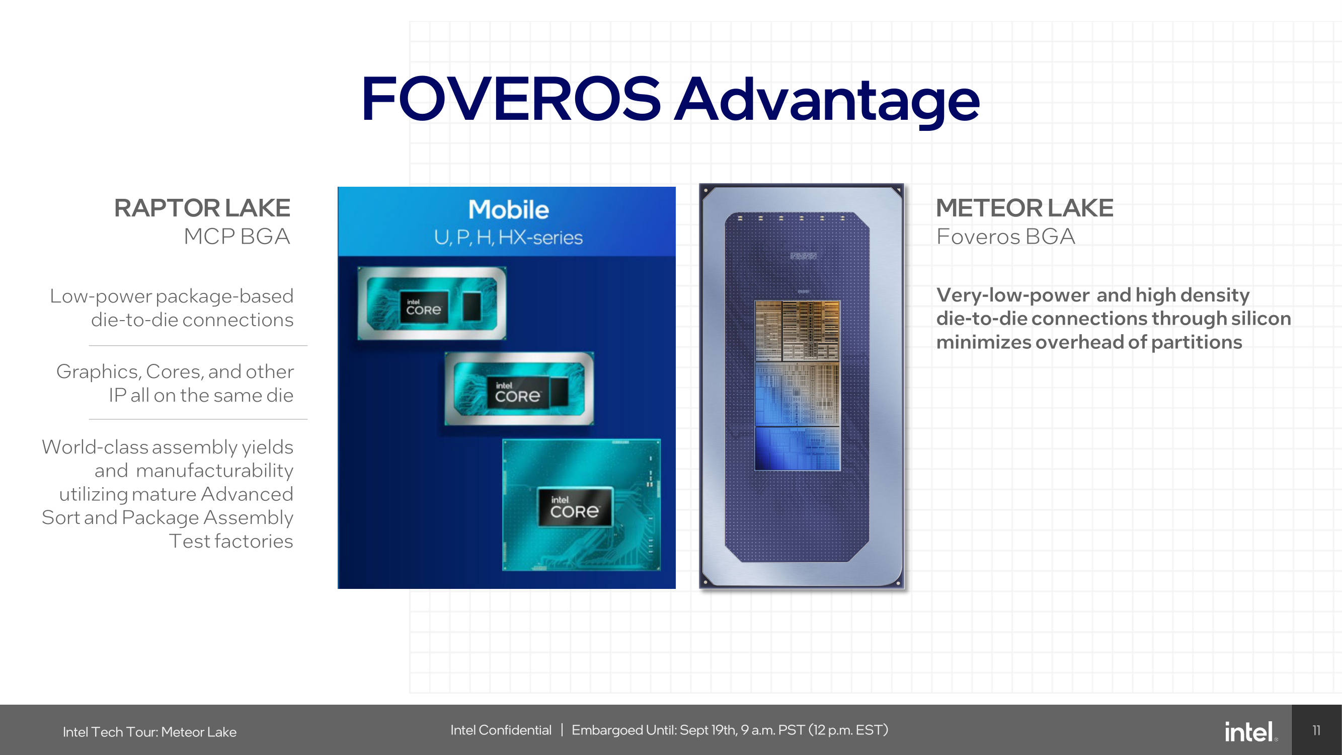
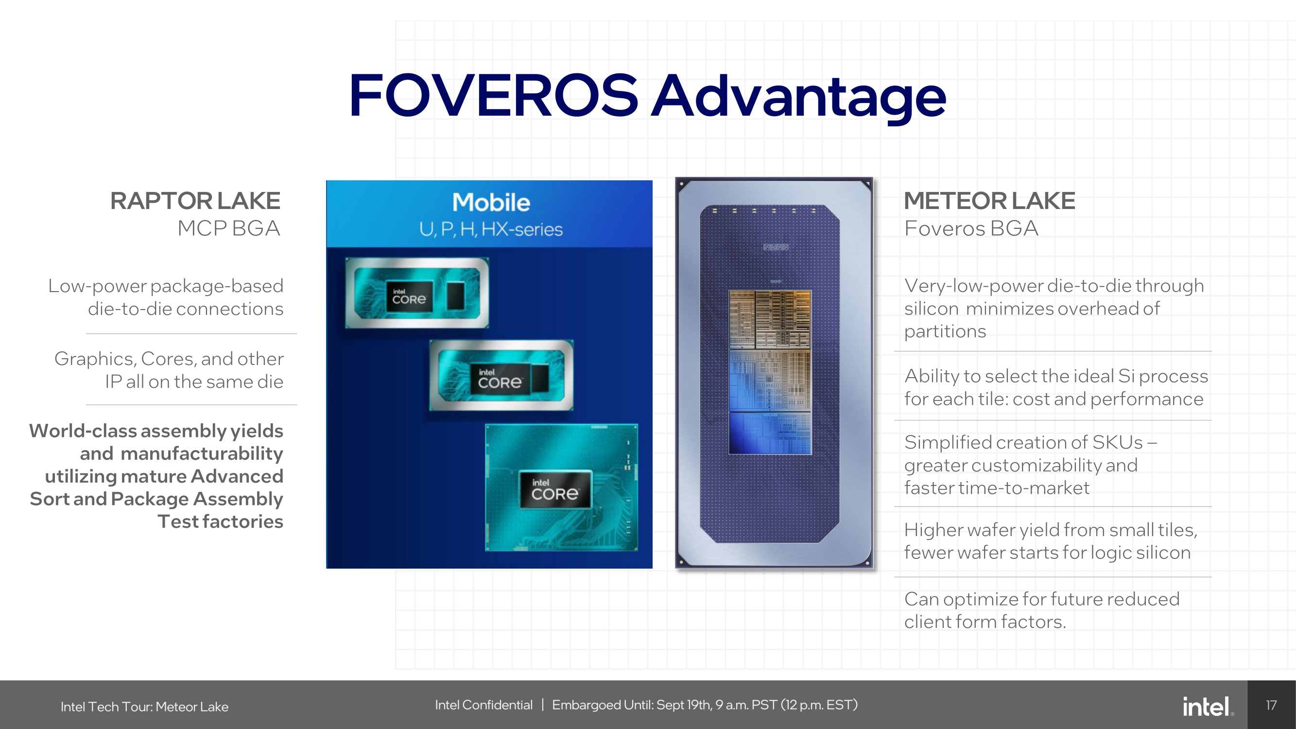
Compared to mobile Raptor Lake, which was done using Multi-Chip Packaging (MCP), Meteor Lake uses Foveros BGA packaging and offers low-power die-to-die interconnects, which Intel confirmed has a small power penalty of between 0.15 and 0.3 picojoules (pJ) communicating from tile to tile. Some of the advantages of Foveros include better customizability through tiling, which allows Intel to manufacture chips and implement specific tiles and IP depending on the grade of the chip, etc., low power with more I/O, or high-end tiles with all the latest gadgets and gizmos. With the Intel 7 node not being as viable as they would have hoped, Intel promises higher wafer yield on Intel 4, which uses less wafer space for logic-based silicon.
Power management is done using a scalable power management system that supports the independent functioning of each tile. Coordination between multiple power management controllers (PMC) and system software is designed to be optimized for various workloads. Intel's Meteor Lake architecture also introduces a new scalable fabric to improve energy efficiency and extend bandwidth in areas that have been previously bottlenecked, such as I/O.
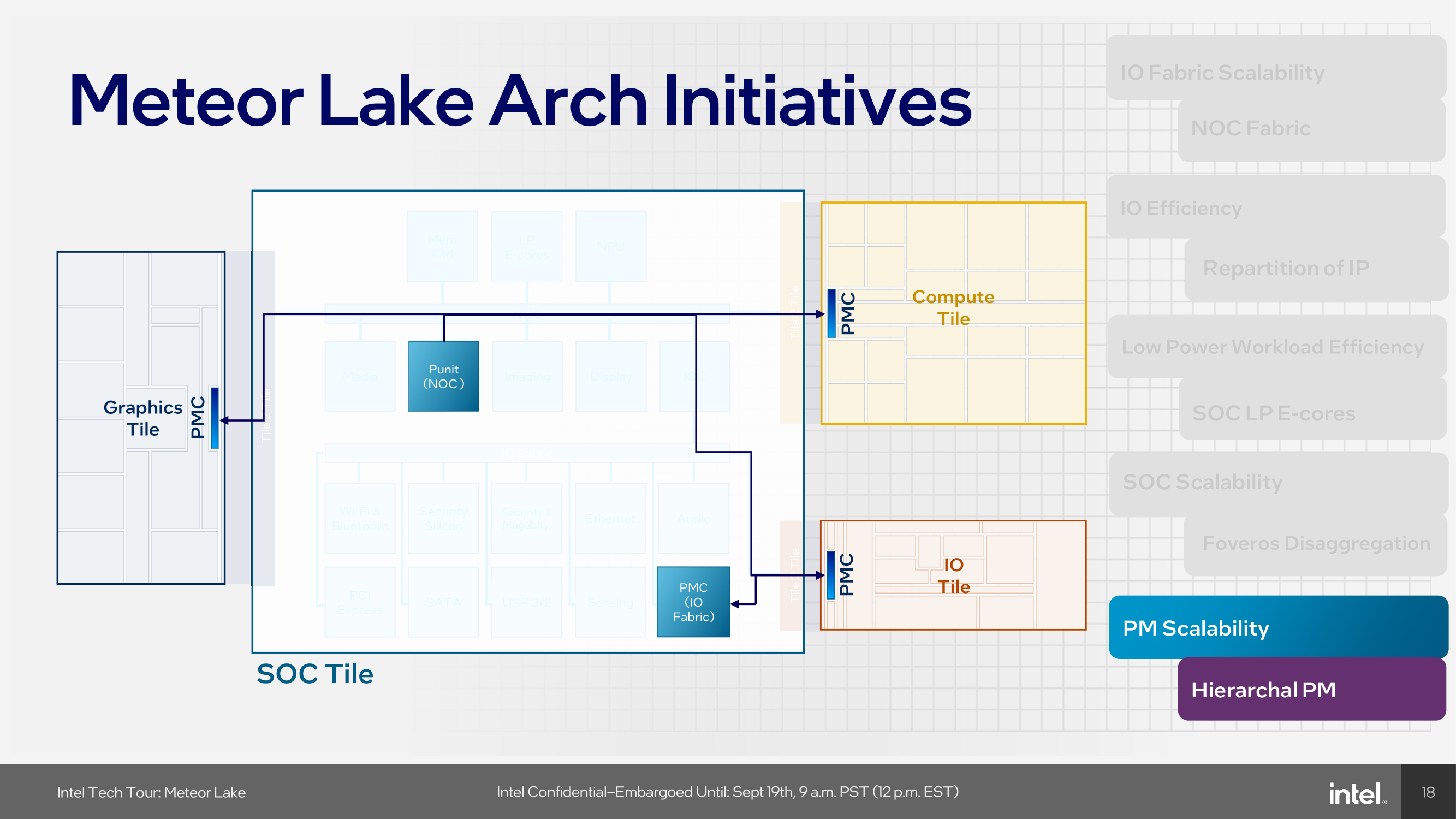
Touching more on the power controllers within the Meteor Lake architecture, Intel has integrated independent Power Management Controllers within each of the tiles. As part of the disaggregation of using Foveros, each tile needs to be independently power managed, and using PMCs on the NOC, the I/O fabric, as well as each tile allows power management to be agnostic depending on the number of the cores on each package.
-16.png)
Meteor Lake itself represents a monumental architectural shift, not just a mere incremental update, as it represents the most significant architectural transformation in client processors in four decades. This is because it's the first client processor to be made using chiplets instead of a monolithic design. The architecture is designed to be the cornerstone of Intel's strategy to push PC innovation for the next decade. Looking at some of the finer details of Intel's Meteor Lake architecture, it uses Intel's Foveros packaging technology, which uses 3D chip stacking to tackle the pitfalls of traditional 2D chip layouts.
-25.png)
As we can see from the above disclosure from Intel at Hot Chips 2023, the top and bottom layers have bumps for interconnecting each die together. Using the Foveros FDI packaging offers a low-voltage complementary metal oxide semiconductor (CMOS) interface, which means the power circuitry can be run with lower voltages and, thus, with a lower power envelope. Another benefit of FDI is both synchronous and asynchronous signaling, which means signal transmission can handle fully duplexed data blocks.
Constructing a Meteor Lake SoC includes a package substrate, which is the foundation for the base tile to sit onto, which uses the Foveros Die Interconnect (FDI). The base tile has a 36µm die to die pitch with metal layering and a 0.15 to 0.3 pJ operating power at 2 GHz; this may fluctuate or vary depending on voltages, amps, and frequency. As it's a base tile that isn't an active chiplet itself, its only function is to serve as a base for all of the various logic, and metal layers for the chiplets to be placed upon.
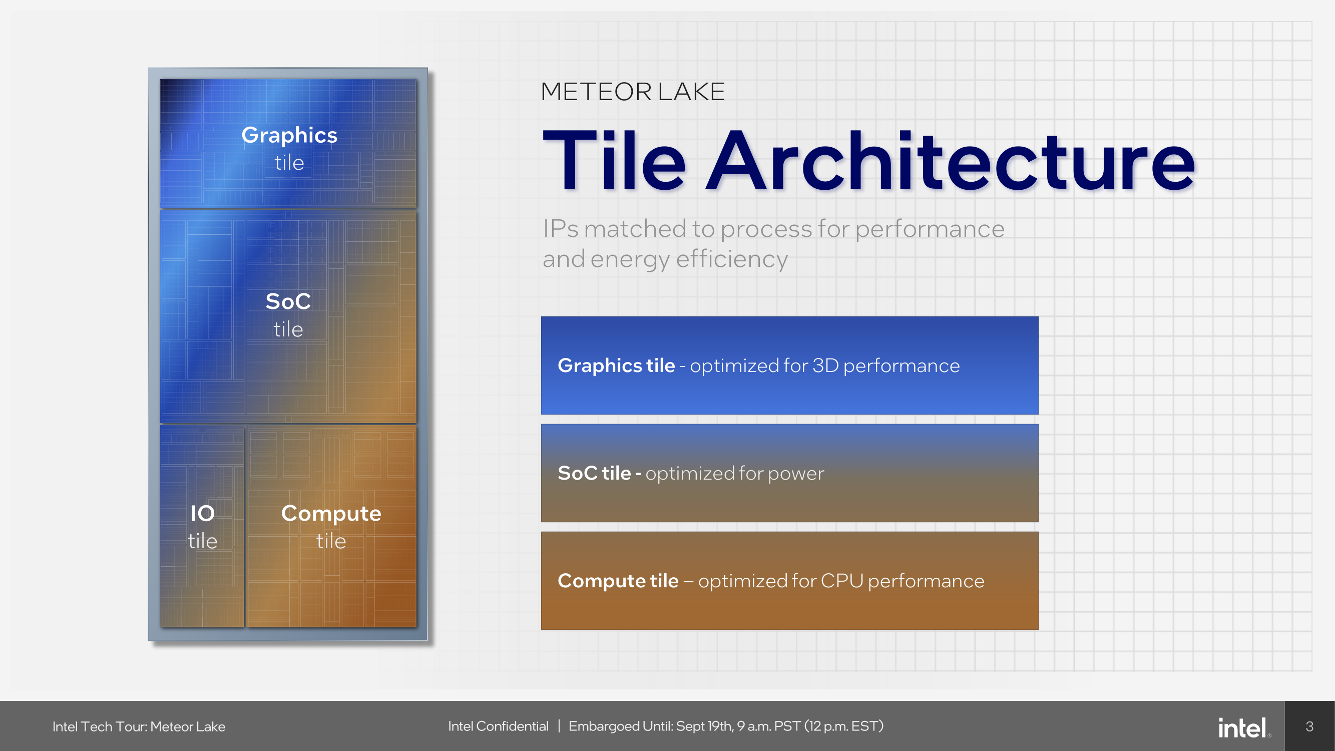
The makeup of Intel's Meteor Lake architecture uses four distinct tiles to create a Meteor Lake CPU. This includes a Compute, SoC, GPU, and an I/O tile, all with distinct uses, capabilities, and flexibility in regard to IP. Power management also gets a revamp. With disaggregation through Intel's Foveros packaging technology, each tile in Meteor Lake requires its own power management. Intel's solution is a hierarchical power management system that uses Power Management Controllers on the NoC, IO fabric, and each individual tile.
Over the next few pages, we'll give an insight into each of the four tiles, what each tile brings to the table, and more about the various technologies driving innovation through Meteor Lake.
Compute Tile: New P (Redwood Cove) and E-cores (Crestmont)
The compute tile is the first client-focused tile to be built on the Intel 4 process technology. It houses the latest-generation P-cores and E-cores, both of which are based on newer and updated architectures. The P-Cores are officially called Redwood Cove, while the E-Cores are Crestmont. Intel also claims that power efficiency is greatly improved from previous generations, combined with its 3D Foveros packaging and offloading less performance-critical elements such as the SoC, media, and graphics onto other tiles. Intel also uses the same ring fabric to interconnect all the tiles to reduce power and latency penalties across the entirety of the chip.
One thing to note with the new core architectures, including Redwood Cove (P-core) and Crestmont (E-core), is that Intel was very light on disclosing many of the finer details. While we got the general blurb of 'it's better than this and has better IPC performance than the last gen,' Intel has omitted details such as L3 cache, whether there's L4 cache through Intel's "Adamintine" hierarchy, and disclosing decoder widths within the cores. As such, Intel hasn't provided enough details for us to do a full architectural deep dive of Redwood Cove or Crestmot, but more an easy look to see what's new and how it's implemented.

Looking at some of the new changes to Meteor Lake, one of the most notable is the introduction of the new Redwood Cove P-core. This new P-core is the direct successor to the previous Golden Cove core found in the 12th Gen Core (Raptor Lake) processors and is designed to bring generational improvements. As expected, Meteor Lake brings generational IPC gains through the new Redwood Cove cores. The Redwood Cove core also has increased bandwidth for both cache and memory. The performance monitoring unit has also been updated to enhance monitoring, and one of the standout features of the new P-Core is the enhanced feedback provided by Intel's Thread Director, which aids in optimizing core performance and directing workloads to the right cores.

Another inclusion is the new Cresmont-based E-cores, which also benefit from generational IPC gains, and they keep the CPU-based AI acceleration through Vector Neural Network Instructions (VNNI) as seen on Raptor Lake (13th Gen) and Alder Lake (12th Gen). Intel claims improvements over the previous gens, although they haven't provided anything to substantiate this.
However, Intel states what it means by improvements: "Architectural simulation vs. Gracemont architecture across a broad set of workloads. VNNI improvements based on doubling the number of VNNI ports. Results may vary." This is a very roundabout way of saying we've doubled the number of AVX2 VNNI ports, but they haven't given us any figures, and with Raptor Lake, not all SKUs had support for the VNNI instruction set. They haven't told us whether or not this is now a feature of the Crestmont E-core itself or if it's, again, SKU-dependent.
This is designed to bolster the user experience when using AI applications and running AI-based workloads, although the NPU on the SoC tile is predominately more suited for these. Like the P-Cores, the E-Cores also benefit from enhanced Thread Director feedback, which provides better granular control and optimization. Workloads that aren't as intensive can be offloaded onto the new Low Power Island E-cores, which are embedded into the SoC tile.

One area where Intel is promising major improvements and optimizations is through Thread Director. The Alder Lake (12th Gen) and Raptor Lake (13th Gen) architecture introduced a nuanced approach to scheduling. Under Alder/Raptor work was assigned a quality-of-service (QoS) ranking, and higher priority work was allocated to P-cores for more demanding and intensive workloads, while lower-ranked workloads are directed to E-cores, primarily to save power.
In cooperation with Microsoft Windows, Intel is bringing new enhancements and refinements into play for Meteor Lake. Meteor Lake's SoC tile LP E-cores represent a third tier of service, and Thread Director will try to keep work there first. Then, if threads need faster performance, they can be moved to the compute tile, accessing the faster, full-power E-cores, and at the top, the P-cores. This gives the chip better overall workload distribution in terms of power efficiency. Moreover, Meteor Lake's strategy to periodically move highly demanding tasks to the P-cores that can benefit from the higher performance levels offers a dynamic approach to thread scheduling.
Overall, this is designed to improve power efficiency through Meteor Lake, giving it more versatility over Raptor Lake regarding task scheduling. The flip side is that, on paper, Meteor Lake is a more efficient platform through these enhancements than Raptor Lake, especially in scenarios requiring rapid adjustments to fluctuating workloads and through those lighter workloads that can be offloaded onto the LP E-cores within the SoC.
Compute Tile: Intel 4 with EUV Lithography
The entirety of the compute tile, including the P and E-cores, is built using the Intel 4 node and is also Intel's first client chip to use EUV lithography. Intel 4 is a key part of Intel's IDM 2.0 strategy, which aims to achieve parity by 2024 and process leadership by 2025. We have already written a piece detailing the Intel 4 node in great detail, which can be found below:
Intel 4 Process Node In Detail: 2x Density Scaling, 20% Improved Performance
Intel 4 uses extreme ultraviolet (EUV) lithography, a highly efficient manufacturing technique that simplifies manufacturing, improving yield and area scaling. Not only is EUV, along with Intel 4, which is designed to scale out for better power efficiency, but it's also the precursor for Intel to switch things over to their Intel 3 process, which is still being developed.

According to Intel's '5 nodes in 4 years' goal within the roadmap, Intel 3 is stated to be manufacturing-ready in H2 of 2023. What's interesting about the cadence of Intel 3 in the roadmap is that Intel 3 is design-compatible with Intel 4, and as such, Intel 3 is designed to be the long-lived node with EUV lithography.

One of the primary benefits of Intel 4 is its area scaling capabilities. The Intel 4 process offers 2X the area scaling for high-performance logic libraries compared with the previous Intel 7 process node – a process which wasn't only troublesome through its exceedingly long development cycle, but yields were not the greatest. Having the ability to scale out in such a way is vital for fitting more and more transistors on a chip, which should theoretically improve the overall performance and efficiency of the silicon. Intel 4 is also optimized for high-performance computing applications and supports both low-voltage (<0.65V) and high-voltage (>1.1V) operations. Intel claims that having this flexibility results in more than 20% performance in iso-power performance over Intel 7, and the technology also incorporates high-density Metal-Insulator-Metal (MIM) capacitors, which Intel claims make power delivery to the chip superior.

Through Intel 4 with EUV, Intel uses a 30 mm fin pitch with self-aligned quad patterning (SAQP) and a 50 nm tungsten gate pitch, scaled down by 0.83x from 54/60 nm on Intel 7. The M0 pitch is also down by 0.75x to 30 nm from 40 nm, and the HP library height has been reduced greatly from 408 in Intel 7 to 240 nm on Intel 4, a scaling of 0.59x. Moving from a 4 fin to 3 fin allocation means that Meteor Lake on Intel 4 has a tighter gate spacing than Intel 7.
One key new introduction to Intel 4 is the materials used, with Intel using what it calls 'Enhanced Copper'. Although Intel hasn't disclosed the specific percentage of the mixture, Enhanced Copper is essentially copper (Cu) adorned with cobalt (Co) and is designed to eliminate high resistance and high volume barriers. The combined metallurgy of copper and cobalt is used on layers M0 to M4, while layers M5 to M15 are made from copper using different pitches ranging from 50 nm up to 280 nm.
| Comparing Intel 4 to Intel 7 | |||
| Intel 4 | Intel 7 | Change | |
| Fin Pitch | 30 nm | 34 nm | 0.88 x |
| Contact Gate Poly Pitch | 50 nm | 54/60 nm | 0.83 x |
| Minimum Metal Pitch (M0) | 30 nm | 40 nm | 0.75 x |
| HP Library Height | 240h | 408h | 0.59 x |
| Area (Library Height x CPP) | 12K nm2 | 24.4K nm2 | 0.49 x |
Using Extreme Ultraviolet (EUV) lithography on Intel 4 represents a major progressive advancement in semiconductor fabrication. Accomplished by using x-rays with a wavelength of around 13.5 nanometers (generated by zapping tin with a laser, no less), EUV lithography significantly improves and optimizes the photolithographic process, allowing for enhanced resolution and pattern fidelity metrology. The technology requires specialized equipment, including high-precision optics and vacuum chambers, with a single EUV lithographic system costing around $150 million (as per Reuters).
When it comes to using manufacturing chips, there are different levels of patterning, both single and multi-patterning. Using EUV allows Intel to reduce the number of masks and steps in the fabrication process, with up to 20% fewer masks on Intel 4 than Intel 7 by replacing multi-patterning steps a single EUV layer. While each patterning level presents its own unique challenges, EUV allows for a single pattern to use just one exposure to etch out. This means that production can be increased and flow faster throughout the process. Opting for multi-patterning means more cost and higher variability. Another advantage of using a single-pattern EUV process also reduces the number of defects within the silicon.
Despite the substantial capital and operational expenditures, the technology offers compelling advantages, such as a reduction in mask count by 20% and a decrease in process steps by 5% for Intel 4. These efficiencies contribute to superior area scaling and yield optimization and put EUV lithography as a cornerstone in Intel's processor roadmap as they try to achieve leadership. It also synergizes with Advanced Packaging Technologies (APT) like Embedded Multi-die Interconnect Bridge (EMIB) and is combined with Foveros 3D packaging, further ensuring its role as a progressive technology in semiconductor and chip manufacturing.
SoC Tile, Part 1: Low-Power Island E-Cores, Designed for Ultimate Efficiency
Diving a little deeper into the SoC tile within Intel's Meteor Lake architecture, Intel hasn't just opted for a minor change but has made a significant leap forward, especially regarding I/O fabric scalability. The SoC tile itself isn't built on Intel 4 like the compute tile but is made by TSMC on their N6 node. Intel has ditched the old limitations of mesh routing by implementing a Network-On-Chip (NOC) on the silicon. This isn't just about making data lanes faster; it's about outlining smarter and more power-efficient access to memory. Likely an innovation from Intel's acquisition of NetSpeed back in 2018, which specialized in NoC and Fabric IP for SoCs, Intel opting for a physical NOC allows Intel to reduce the limits on bandwidth. Using EMIB and the nature of 2D scaling, the data paths are a lot shorter, translating into less power loss, but shorter wires also help reduce overall latency penalties.

Switching gears to low-power workload efficiency, Meteor Lake incorporates E-cores directly into the SoC tile, which Intel calls Low Power Island (LP) E-cores. Think of it as Intel's way of saying, "Why use a sledgehammer when a scalpel will do?". This means that the LP E-Cores are driven purely from a power-saving perspective. Having these LP E-cores available for workloads with the aid of Intel's Thread Director means lighter threads and background tasks that don't require the grunt of the P and E-cores on the compute tile can be directed onto the lower-powered LP E-cores.

While both the E and LP E-cores are based on the same Crestmont microarchitecture, the E-cores on the compute tile are built on Intel 4, along with the P-cores. The LP E-cores are made on TSMC's N6 node, like the rest of the SoC tile. These low-power island E-cores are tuned for finer-grained voltage control through an integrated Digital Linear Voltage Regulator (DLVR), and they also have a lower voltage-to-frequency (V/F) curve than the big E-cores on the compute tile, meaning they can operate with a lower power cost, thus saving power when transitioning low-intensity workloads off of the compute tile and onto the LP E-cores.
Part of the disaggregated nature of Foveros combined with individual power management controllers (PMC) within each tile means that IP blocks can be independently powered on or off when required.
SoC Tile: Bandwidth Scalability, Can't Stop The NOC
So adding a variety of tiles requires a highly competent pathing to ensure bandwidth is adequately structured. As I/O bandwidth bottlenecking was a major concern in previous iterations, Intel aims to solve bandwidth flow restrictions with a couple of solutions.

The first is through the scalability of the I/O bandwidth, which Intel does by adding what it calls 'Scalable Fabric,' which is configured for up to 128 GB/s of bandwidth throughput. All of the I/O ordering and address translation is fed through the IOC, while Intel has implanted a Network-on-Chip (NOC) to interconnect many of the different areas of the SoC.
The Network-on-Chip or NOC is designed to be coherent, and for Meteor Lake on Intel 4, this uses unordered processing, which moves data in an unordered fashion. Connecting all the tiles together through the NOC and independently through the IOC gives plenty of bandwidth headroom for devices or agents requiring it. The NOC is directly connected to the compute and graphics tile, while other elements, including the traffic fed directly through the LP E-cores on the SoC tile, media, display, the NPU, and the imaging processing unit (IPU), all going through the NOC. In terms of the connection to the I/O tile, this is connected directly to the IO fabric and then is fed through the IOC, which then goes directly to the NOC.
The SoC tile also integrates Wi-Fi 6E and can be made to support the latest Wi-Fi 7 standard. Having a future-proof method of including Wi-Fi 7 and Bluetooth 5.4 can add the next level of wireless connectivity to Intel's mobile platform. Wi-Fi 7 offers 320 MHz of bandwidth, doubling the channel width compared to its predecessor, Wi-Fi 6. It also uses 4096-QAM (4K QAM) to enable transmission speeds capable of hitting 5.8 Gbps.
We're still waiting for clarification on what this actually means. Whether it's supportive of Wi-Fi 7 or if there's some underlying compatibility within the Wi-Fi MAC integrated into the silicon. One option could be that Intel is adding a full external controller into the silicon to get to Wi-Fi 7 instead of CNVio splitting up parts of the radio stack. We have asked Intel for more details and will update you when we have a response.
That being said, Intel discloses 'support' for Wi-Fi 7 and BT 5.4, but there's a chance Intel could differentiate which wireless MAC is implemented into different chip segments. An example would be an Intel 9 Ultra SKU, bolstered by Wi-Fi 7 support, whereas a lower-end SKU like a Core 3 might utilize Wi-Fi 6E to save on cost.
Additional features include Multi-Resource Unit (RU) Puncturing and Military-grade security with WPA3 that supports GCMP-256 encryption to ensure both speed and security when connected to a wireless network. Unique features like Multi-Link Operation (MLO) in Wi-Fi 7 are designed to reduce latency and jitter by up to 60%, making it a competent solution for various user's connectivity needs. Adding Bluetooth 5.4 further complements this by improving audio quality, and it is claimed to offer up to 50% lower power consumption for longer battery life.

Also present on the SoC tile is the display controller and the media engine from the GPU. These are always-on (or at least, mostly-on) blocks that do not need to be built on a cutting-edge process node, making them good candidates to place on the SoC tile. Meteor Lake offers support for 8K HDR and AV1 video playback and contains native HDMI 2.1 and DisplayPort 2.1 connectivity.
Finally, the SoC tile also includes other key platform components, such as PCIe lanes, which are integral for connectivity to external devices such as discrete graphics cards and the platform's I/O capabilities, such as USB 4 and 3, as well as offering a direct interconnect to a separate I/O tile with Thunderbolt 4 and additional PCIe lanes. While we've touched on wireless connectivity, the SoC tiler also includes Ethernet support, although Intel hasn't disclosed yet which PHY will be included; it is likely to be capable of 2.5 GbE at the minimum.
A Note on Meteor Lake's Security Features: New Silicon Security Engine (ISSE)
Security has also been given closer attention in Meteor Lake. The architecture introduces the Intel Silicon Security Engine (ISSE), a dedicated component focused solely on securing things at a silicon level. Various vulnerabilities have been at the forefront of media over the last few years, including Meltdown, Spectre, and Foreshadow.

With real threats around the world, securing data is ever prevalent, and CPU architects and designers not only need to consider performance and efficiency, but security and doing some architecturally is just as important as a competent software stack. The Converged Security and Manageability Engine (CSME) has also been partitioned to further enhance platform security. These features collectively work to give a wide range of on-chip and off-chip securities designed to mitigate attacks on multiple fronts.
SoC Tile, Part 2: NPU Adds a Physical AI Engine
The last major block on the SoC tile is a full-featured Neural Processing Unit (NPU), a first for Intel's client-focused processors. The NPU brings AI capabilities directly to the chip and is compatible with standardized program interfaces like OpenVINO. The architecture of the NPU itself is multi-engine in nature, which is comprised of two neural compute engines that can either collaborate on a single task or operate independently. This flexibility is crucial for diverse workloads and potentially benefits future workloads that haven't yet been optimized for AI situations or are in the process of being developed. Two primary components of these neural compute engines stand out: the Inference Pipeline and the SHAVE DSP.

The Inference Pipeline is primarily responsible for executing workloads in neural network execution. It minimizes data movement and focuses on fixed-function operations for tasks that require high computational power. The pipeline comprises a sizable array of Multiply Accumulate (MAC) units, an activation function block, and a data conversion block. In essence, the inference pipeline is a dedicated block optimized for ultra-dense matrix math.
The SHAVE DSP, or Streaming Hybrid Architecture Vector Engine, is designed specifically for AI applications and workloads. It has the capability to be pipelined along with the Inference Pipeline and the Direct Memory Access (DMA) engine, thereby enabling parallel computing on the NPU to improve overall performance. The DMA Engine is designed to efficiently manage data movement, contributing to the system's overall performance.

At the heart of device management, the NPU is designed to be fully compatible with Microsoft's new compute driver model, known as MCDM. This isn't merely a feature, but it's an optimized implementation with a strong emphasis on security. The Memory Management Unit (MMU) complements this by offering multi-context isolation and facilitates rapid and power-efficient transitions between different power states and workloads.

As part of building an ecosystem that can capitalize on Intel's NPU, they have been embracing developers with a number of tools. One of these is the open-source OpenVINO toolkit, which supports various models such as TensorFlow, PyTorch, and Caffe. Supported APIs include Windows Machine Learning (WinML), which also includes the DirectML component of the library, the ONNX Runtime accelerator, and OpenVINO.

One example of the capabilities of the NPU was provided through a demo using Audacity during Intel's Tech Tour in Penang, Malaysia. During this live demo, Intel Fellow Tom Peterson, used Audacity to showcase a new plugin called Riffusion. This fed a funky audio track with vocals through Audacity and separated the audio tracks into two, vocals and music. Using the Riffusion plugin to separate the tracks, Tom Peterson was then able to change the style of the music audio track to a dance track.
The Riffusion plugin for Audacity uses Stable Diffusion, which is an open-source AI model that traditionally generates images from text. Riffusion goes one step further by generating images of spectrograms, which can then be converted into audio. We touch on Riffusion and Stable Diffusion because this was Intel's primary showcase of the NPU during Intel's Tech Tour 2023 in Penang, Malaysia.

Although it did require resources from both the compute and graphics tile, everything was brought together by the NPU, which processes multiple elements to spit out an EDM-flavored track featuring the same vocals. An example of how applications pool together the various tiles include those through WinML, which has been part of Microsoft's operating systems since Windows 10, typically runs workloads with the MLAS library through the CPU, while those going through DirectML are utilized by both the CPU and GPU.

Other developers include Microsoft, which uses the capability of the NPU in tandem with the OpenVINO inferencing engine to provide cool features like speech-to-text transcripts of meetings, audio improvements such as suppressing background noise, and even enhancing backgrounds and focusing capabilities. Another big gun using AI and is supported through the NPU is Adobe, which adds a host of features for adopters of Adobe Creative applications use. These features include generative AI capabilities, including photo manipulative techniques in Photoshop such as refining hair, editing elements, and neural filters; there's a lot going on.
SoC Tile, Part 3: Disaggregating Xe Media and Display Engine From Graphics
As we noted earlier, Intel has completely redesigned its graphics, media, and display engine for Meteor Lake and, as such, separates all three entities from each other. While we'll cover the new graphics tile next, we'll start with everything that's not part of the graphics tile. Opting for a disaggregated architecture allows Intel to not only shuffle things around from an IP perspective but also allows Intel to integrate new IPs such as cores, graphics, and I/O as and when advancements have been made at a silicon level, but the design allows unties Intel from being limited to a specific manufacturing process.

Starting things off, we have the Xe Media Engine, which is embedded within the SoC tile. Within the Xe Media Engine are two Multi-Format Codecs (MFX), designed and responsible for all the encoding and decoding tasks. Intel's Meteor Lake with Xe supports the latest codecs ranging from AV1 (decode and encode), HEVC, AVC, and VP9, with up to 8K60 HDR decode supported. For encoding, there's support for up to 8K resolutions with 10-bit color and HDR. Aiming to improve power efficiency on-chip with encode/decode workloads, having a dedicated Media Engine separate from the graphics allows Intel to find granular power savings as things are directed to the Xe Media Engine, which means the graphics tile doesn't need to be powered up to accomplish encode or decode tasks.

The Xe Media Engine provides various functionalities across a large spectrum of different video codecs. This ranges from JPEG/MPEG and AVC to the more advanced VP9, HEVC, and AV1 codecs. Designed to give Meteor Lake a solid level of computational efficiency for video processing, the Xe Media Engine balances the gaps between high-performance output and power efficiency, rendering it particularly well-suited for various applications, from real-time video streaming to high-fidelity playback. There's also support for diverse color formats and bit depths, including but not limited to 4:2:0 at 10-bit and 12-bit, which means it's versatile for video editing and video encoding and should satisfy content creator's needs.
Xe Display Engine: Also Within the SoC
Much like the Xe Media Engine, the Xe Display Engine is also found within the SoC tile on Meteor Lake. Decoupling this directly from the graphics tile and embedded into the SoC allows it to communicate directly with the Xe Media Engine, saving power and improving overall battery life. The engine supports up to four display pipes, two of which have been designed and optimized for low power consumption, further boosting overall efficiency for Meteor Lake.

Looking at compatibility, the Xe Display Engine looks to use the latest connections and ports, including native support for HDMI 2.1, DisplayPort 2.1, Embedded DisplayPort (eDP) 1.4. and even DSC 1.2a. Via these blocks, Meteor Lake can support displays up to 8K60 HDR, or up to 4 x 4K60 HDR displays, and this is on top of 1080p360 and 1440p360 too. This gives Meteor Lake substantial display and multimedia device support, including current and up-and-coming panels.
I/O Tile: Extended and Scalable Depending on Segment
The smallest of Meteor Lake's tiles is the I/O tile, which is primarily designed to offer additional connectivity features. This, of course, is down to two things; specific vendor's needs and the grade of processor itself. As Meteor Lake is scalable, the I/O tile is perhaps the crux of enabling specific features such as Thunderbolt 4 on devices. A lower-end Intel Core 3 Meteor Lake chip is likely to drop flashy I/O-specific features such as TB4 to save on cost, as entry-level notebooks aren't going to use it.
-20.png)
The higher end of the Meteor Lake product stack will feature Thunderbolt 4, and although it will be on the I/O tile for notebook vendors to utilize, having a scalable I/O fabric allows Intel to implement a modular approach to I/O features instead of one that is more one size fits all. The I/O tile includes additional PCIe lanes, but this number will vary depending on the processor itself; a higher-end chip will have more for additional storage needs, whereas a lower-end chip will have the minimum for connectivity and whatnot. Something else is that the I/O tile isn't a PCIe Coherent Fabric, which means data can only be transferred without the support for cache coherency between memory and devices.
Graphics Tile: A Generational Leap Through Arc, Xe-LPG Graphics
As part of their disaggregated architecture for Meteor Lake, Intel has opted to use a separate tile for graphics. Intel has gone down an interesting route for its disaggregated graphics, with the most notable inclusion through an upgrade to Intel's Arc Graphics architecture. Powering Intel's integrated graphics for Meteor Lake is a new graphics architecture which Intel calls Xe-LPG (and no, we're not talking about fuel here). Based on Intel's current discrete graphics architecture known as Xe-HPG (used in their Arc GPUs), Intel claims 2x performance per watt compared to the Xe-LP architecture-based Iris Xe integrated graphics within Intel's 12th Gen Core series.
There are a number of different elements within the graphics and media area of Meteor Lake, the bulk of which is built into the graphics tile, where the Xe-LPG graphics architecture is located. Unlike the compute tile (Intel 4) and the SoC tile, which is manufactured on TSMC N6 (6 nm), the graphics tile is made on TSMC's N5 node (5 nm), the same generational family as the nodes used by AMD and NVIDIA's discrete and integrated GPUs.

With Meteor Lake and the graphics tile with the Xe-LPG graphics processor, Intel is promising discrete-level performance in an integrated form factor. Looking at the finer specifications, Intel includes 8 x Xe graphics cores with 128 vector engines (12 per Xe core) and 8 samplers, representing a 1.33 x increase over Intel's previous Xe LP graphics. There are also 4 Pixel backends, which is an improvement over the 3 PBs on Xe LP. Intel also doubles the number of geometry pipelines within Xe-LPG, with two, and they also introduce 8 dedicated Ray Tracing Units (RTU), which is new for Intel's integrated graphics line-up.

Looking at the makeup of Intel's Xe core, as previously mentioned, there are 16 Vector Engines that have a bus width of 256-bit, while each core also has 192 KB of shared L1 cache. Each Vector Engine enables 16 FP32 ops per clock, and 32 FP16 ops per clock, with a shared FP64 execution port with 64 INT8 ops per clock. One dedicated FP64 ops per clock unit is new over what's previously been seen in Raptor Lake and shares the overall design philosophy of Meteor Lake on power efficiency; pairs of Vector Engines can run in lockstep for better efficiency.
As part of Intel's goal of advancing the overall experience with Xe-LPG for users, the graphics are DX12 optimized, and Intel now brings Out of Order Samplng (OoOS) to Xe-LPG. It's worth noting that when talking about Execution Units (EUs), Intel's new and current term for this is Xe Vector Engines, or XVE for short. Intel hasn't provided us with how OoOS works within Xe-LPG, but we've reached out for more details.
| Comparing Intel Xe Integrated Graphics (Mobile) | ||||
| Meteor Lake (Xe-LPG) |
Raptor Lake (Xe-LP) |
Alder Lake GT1 (Xe-LP) |
Tiger Lake GT2 (Xe-LP) |
|
| Process Node | TSMC N5 | Intel 7 | Intel 7 | Intel 7 |
| Vector Engines/EUs | 128 | 96 | 96 | 96 |
| ALUs/Shaders | 1024 | 768 | 768 | 768 |
| TMUs | ?* | 48 | 16 | 48 |
| ROPs | ?* | 24 | 8 | 24 |
| Ray Tracing Units | 8 | - | - | - |
| TDP | ? | 15 W | 15 W | 15 W |
*Intel hasn't given us a deep dive into the finer specifications of Xe-LPG integrated graphics. Looking at an existing integrated Intel Arc equivalent with similar specs, the Meteor Lake Xe LPG could have 64 TMUs and 32 ROPs per the Arc A370M, which also has 1024 ALUs.
Comparing Intel's integrated Xe graphics from previous mobile architectures, Meteor Lake, through the Xe-LPG Arc based graphics, has 128 XVEs, which is an increase of 1.33 X or 32 XVE/EUs, than the previous Xe-LP generation. Regarding arithmetic logic units (ALUs), which are essentially shader cores, Xe-LPG has been increased to 1024, which is 128 ALUs per Xe-LPG core. As previously mentioned, Intel hasn't given us more about the finer specifications, including TMUs or ROPs, but does bring 8 Ray Tracing units, which is new for Xe-LPG when compared directly to Xe-LP.
Meanwhile, with Intel's Foveros 3D packaging technology, disaggregating the Media Engine and Display Engine from the graphics tile means when doing encoding or decoding, as well as video playback, it doesn't require the graphics tile to be powered up to do workloads on more power consuming cores.

Intel Xe-LPG is the next step up from Xe LP, and one area where performance and efficiency gains are made is through a lower voltage frequency (V/F) curve, allowing the graphics to run at a lower minimum voltage with a higher maximum core clock speed. Intel has also optimized the pipelines for faster frequencies and is claiming up to 2 x performance at iso-voltages, which for a mobile platform such as Meteor Lake, adds more potential with a key focus on achieving a figure of up to 20% in power savings compared to the previous generation.
Intel Meteor Lake: Changing The Strategy, Laying the Foundation for Intel 3
The strategy for both the Intel 4 process and the first architecture built on it, Meteor Lake, looks to change the dynamic for the mobile market and the foreseeable future of Intel's client processors. With the Foveros 3D packaging, opting for a power-conscious mobile platform seemed the best way to showcase their gains in terms of power efficiency.
One of the main product assembly advantages of Foveros packaging is that Intel can chop and change tiles depending on the processor, which includes current technologies, I/O, graphics, and compute cores. This approach to 3D tiled packaging also means that it is theoretically easier to introduce new tiles with faster cores with higher IPC performance, new graphics processors, and newer I/O, such as Wi-Fi 7. With Foveros not limiting Intel to use a single, monolithic die, it allows Intel to use different manufacturing processes for each of the tiles and integrate them onto the silicon. This is prevalent with the compute tile being built on Intel 4, while the graphics tile in Meteor Lake is made using TSMC's N5 node. This flexibility is key to advancing innovation, customizability, and, of course, wafer yield.
-24.png)
Intel Meteor Lake from Hot Chips Slide Deck
Intel also introduced a dedicated in-silicon AI engine through the NPU within the SoC tile. Similar to AMD with their Ryzen AI technology, Intel is looking to capitalize on the AI rush within its client-focused processors, but with support for OpenVINO and also including MCDM driver-compliance, users can do some pretty cool things with AI inferencing on the chip. Although these implementations aren't akin to the types of AI inferencing done in the cloud via ChatGPT with dedicated AI hardware, it's a step in the right direction in a world that looks to be slowly taken over by AI.
-35.png)
Wrapping things up, while Intel is confirming that Meteor Lake is coming to mobile-first, any details beyond that are slim pickings. At this point in time, Intel hasn't revealed anything in regard to SKUs or possible configurations. Everything disclosed is based on the 'full; Meteor Lake processors, but Intel hasn't spoken about different configurations or what the lower-end segment might look like regarding tiles and implementations. From their Hot Chips disclosures, offering a tiled architecture allows them to scale upwards and down depending on the SKU. The high-end SKU, which hasn't been disclosed yet, will feature the full configuration and implementation of all the features. Otherwise, the scalable nature of Meteor Lake and disaggregation allows for different levels of compute and graphics tiles and the ability to scale the input and output (I/O) depending on the device.
Meteor Lake will also be the first mobile platform from Intel to use their new Core naming scheme for products, which drops the 'i' from the Core branding. This includes the Core 3, 5, and 7, as well as higher spec Ultra 5, 7, and 9 Ultra tiers. Pat Gelsinger, Intel's Chief Executive Officer (CEO), during his opening keynote at Intel Innovation 2023, states that Intel is launching the first Meteor Lake Ultra (high-end) SKU with AI capabilities (NPU) on December 14th.

A tray of Meteor Lake Core Ultra processors (Credit, Intel)
We expect Intel to disclose more about specific SKUs and other specifications, such as clock speeds and core configurations, as we get closer to Meteor Lake's launch. Although we're expecting Ultra-focused Meteor Lake SKUs to launch on December 14th, no details on when we can expect other SKUs are set to hit retail channels. Meteor Lake is likely to launch with the top Ultra SKU or at least one that is close to the top of the stack.
Reading the tea leaves ahead of Innovation 2023, one gets the impression that Intel was hoping to be just a bit closer to launch by now than they actually are. But all things will eventually come in due time...


