Intel High-NA Lithography Update: Dev Work On Intel 18A, Production On Future Node
by Ryan Smith on September 20, 2023 7:20 PM EST
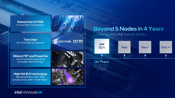
As part of Intel’s suite of hardware announcements at this year’s Intel Innovation 2023 conference, the company offered a brief update on their plans for High-NA EUV machines, which will become a cornerstone of future Intel process nodes. Following some changes in Intel’s process roadmap – in particular Intel 18A being pulled in because it was ahead of schedule – Intel’s plans for the next-generation EUV machines. Intel will now only be using the machines with their 18A node as part of their development and validation work of the new machines; production use of High-NA machines will now come on Intel’s post-18A node.
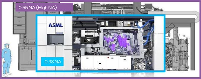
High Numerical Aperture (High-NA) machines are the next generation of EUV photolithography machines. The massive scanners incorporate 0.55 numerical aperture optics, significantly larger than the 0.33 NA optics used in first-generation production EUV machines, which will ultimately allow for higher/finer quality lines to be etched. Ultimately, High-NA machines are going to be a critical component to enabling nodes below 2nm/20 angstroms.
At the time that Intel laid out their “5 nodes in 4 years” roadmap in 2021, the company announced that they were going to be the lead customer for ASML’s High-NA machines, and would be receiving the first production machine. High-NA, in turn, was slated to be a major part of Intel’s 18A node.

Size Comparison: ASML Normal & High NA EUV Machines
But since 2021, plans have changed for Intel, seemingly in a good way. Progress on 18A has been ahead of schedule, such that, in 2022, Intel announced they were pulling in 18A manufacturing from 2025 to H2’2024. Given that the release date of ASML’s High-NA machines has not changed, however, that announcement from Intel left open some questions about how High-NA would fit into their 18A node. And now we finally have some clarification on the matter from Intel.
High-NA machines are no longer a part of Intel’s production plans for 18A. With the node now arriving before production-grade High-NA machines, Intel will be producing 18A with the tools they have, such as ASML’s NXE 3000 series EUV scanners. Instead, the intersection between 18A and High-NA will be that Intel using the 18A line to develop and validate the use of High-NA scanners for future production. After which, Intel will finally use High-NA machines as part of the production process for their next-generation, post-18A node, which is simply being called “Intel Next” right now.
As for the first High-NA development machine, Intel also confirmed this week that their schedule for development remains on track. Intel is slated to receive their first High-NA machine late this year – which as Pat Gelsinger put it in his keynote, is his Christmas present to Dr. Ann Kelleher, Intel’s EVP and GM of technology development.
Finally, back on the subject of the Intel 18A process, Intel says that they are progressing well on their second-generation angstrom node. The 0.9 PDK, which should be the final pre-production PDK, is nearly done, and should enable Intel’s teams to ramp up designing chips for the process. Intel, for its part, intends to start 18A silicon fab work on Q1’2024. Based on Intel’s roadmaps thus far, that is most likely going to be the first revision of one of the dies on Panther Lake, Intel’s first 18A client platform.


_575px.JPG)


24 Comments
View All Comments
FunBunny2 - Sunday, September 24, 2023 - link
house those machines. (They're 3 stories tall!)wait... so industry needs ever huger machines to make ever smaller chips? Kafka should sue for copyright infringement. Reply
m53 - Thursday, September 21, 2023 - link
The number of people just dismissing Intel is baffling. Is it really that improbable that the semiconductor process leader for most of the history can take back the lead again. It's not that TSMC never had process issues. ReplyDante Verizon - Friday, September 22, 2023 - link
Intel broke the record for failures among all large corporations. ReplyJorgp2 - Friday, September 22, 2023 - link
Huh?AMD was on bulldozer for nearly 7 years, and it almost bankrupted them Reply
Dante Verizon - Saturday, September 23, 2023 - link
It may be attributed in part to shady anti-competition tactics by Intel. But this is a single case, Intel, being much larger, failed countless times and in several markets (GPU, Memory, Nand, Smartphones, etc.), and ended up losing tens of billions in the process.Skepticism is justifiable, especially when Intel intends to continue manufacturing GPUs at TSMC. Reply
whatthe123 - Saturday, September 23, 2023 - link
bulldozer wasn't because of intel. they got a huge cash injection from the global foundries spinoff to design bulldozer, all thanks to the antitrust win.opteron failing was because of intel. Reply
FunBunny2 - Sunday, September 24, 2023 - link
Intel broke the record for failures among all large corporations.well... this dispute comes down to tooling, which is ASML sole sourced for this step (much of the rest from other vendors as well). to put the blame on Intel's tooling assumes that a significant %-age of said tooling is made by Intel. any notion how much of such tooling is bespoke to Intel, or TSMC, or etc.? and how much is just bad arch and micro-arch? a craftsman never blames his tools. Reply
JKflipflop98 - Friday, September 22, 2023 - link
Indeed. It's like these kids forgot the last 50 years. ReplyTristanSDX - Thursday, September 21, 2023 - link
Intel propaganda: unquestioned leadership, process / cpu ahead of shedule, PDK almost ready, better than expected, no roadblocks ahead...Then they release Raptor Lake Refresh Reply
Anymoore - Friday, September 22, 2023 - link
One logistic issue with High-NA EUV is stitching; some lines may be exposed in two parts, with breaks or shifts across boundaries.Thinner resists are needed.
And there's a hole in one of the mirrors (troublesome for light to avoid). Reply